ASML says customers are already placing orders for advanced chipmaking tools years in advance, with AI-driven semiconductor demand remaining strong enough to strain capacity despite planned expansions
TSMC’s management confirms that the company is looking forward to expand U.S. capacity beyond Arizona and Texas is one of its options. However, to become a part of the Terafab project, it insists on running the whole fab.
Russian semiconductor players shows off bespoke CPU and SoC designs — Arm and Elbrus architectures on display
Two workers have died in an explosion at Intel’s Kiryat Gat chip plant; police suspect a gas cylinder malfunction.
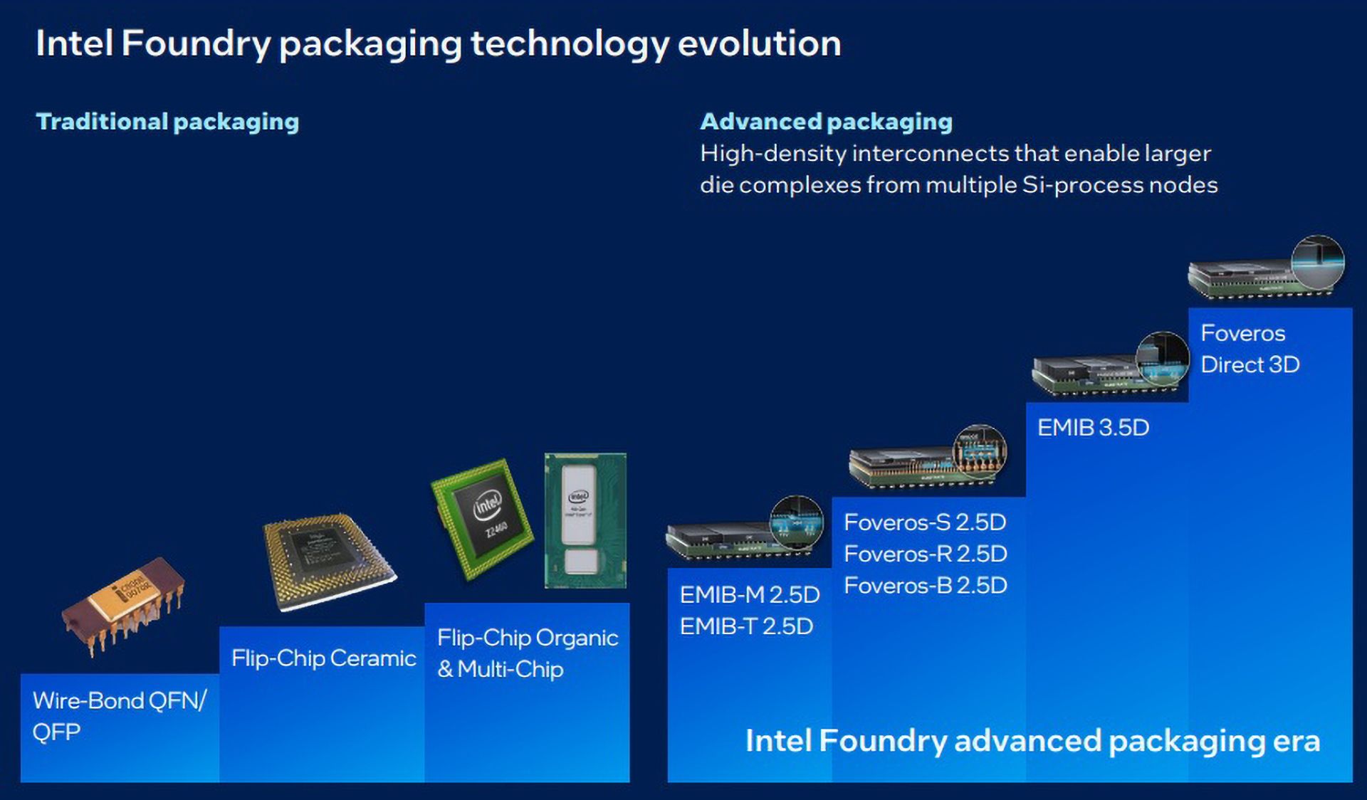
Intel was the first large chipmaker to start using advanced packaging methods in 2017 – 2019. But where are Intel’s EMIB and Foveros technologies today and where are they heading?
Elon Musk may prefer FEL light sources for in-house chip production, but Terafab will start with proven tech from ASML.
Broadcom chief executive Hock Tan compared many AI investors to gamblers who have little idea what they are betting on. He spoke on Monday at the DBS Asia Future Forward Conference in Singapore, Bloomberg reported. “A lot of investors have no clue what…
Amazon is in talks to buy the AI startup Decart in a deal that could value it at about $7bn, The Wall Street Journal reported on Sunday. Kate Clark and Lauren Thomas reported the talks, citing people familiar with the matter. A deal could come soon if …
GlobalFoundries returns to advanced FD-SOI development with 7nm-class FDX Fusion process — production planned for 2028.
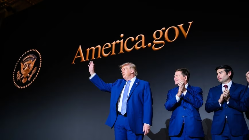
Six technology leaders received the country’s highest honours for science and technology from President Donald Trump on Thursday, the White House said. Elon Musk, Sergey Brin, Jensen Huang and Lisa Su got the National Medal of Science. Michael Dell and…